- English
- French
- German
- Portuguese
- Spanish
- Russian
- Japanese
- Korean
- Arabic
- Greek
- German
- Turkish
- Italian
- Danish
- Romanian
- Indonesian
- Czech
- Afrikaans
- Swedish
- Polish
- Basque
- Catalan
- Esperanto
- Hindi
- Lao
- Albanian
- Amharic
- Armenian
- Azerbaijani
- Belarusian
- Bengali
- Bosnian
- Bulgarian
- Cebuano
- Chichewa
- Corsican
- Croatian
- Dutch
- Estonian
- Filipino
- Finnish
- Frisian
- Galician
- Georgian
- Gujarati
- Haitian
- Hausa
- Hawaiian
- Hebrew
- Hmong
- Hungarian
- Icelandic
- Igbo
- Javanese
- Kannada
- Kazakh
- Khmer
- Kurdish
- Kyrgyz
- Latin
- Latvian
- Lithuanian
- Luxembou..
- Macedonian
- Malagasy
- Malay
- Malayalam
- Maltese
- Maori
- Marathi
- Mongolian
- Burmese
- Nepali
- Norwegian
- Pashto
- Persian
- Punjabi
- Serbian
- Sesotho
- Sinhala
- Slovak
- Slovenian
- Somali
- Samoan
- Scots Gaelic
- Shona
- Sindhi
- Sundanese
- Swahili
- Tajik
- Tamil
- Telugu
- Thai
- Ukrainian
- Urdu
- Uzbek
- Vietnamese
- Welsh
- Xhosa
- Yiddish
- Yoruba
- Zulu
What Is a Planar Titanium Target and How Is It Used?
Planar titanium targets are essential components in various thin-film deposition processes, particularly in physical vapor deposition (PVD) applications. These high-purity, precision-engineered discs or plates of titanium serve as the source material for creating thin films on substrates through sputtering techniques. Planar titanium targets are widely used in industries such as semiconductors, optics, and advanced materials manufacturing due to their unique properties and versatility. The targets are typically made from high-grade titanium, often with purities exceeding 99.995%, and are carefully machined to ensure uniformity in thickness, surface finish, and microstructure. This level of precision is crucial for achieving consistent and high-quality thin film deposition, which is paramount in the production of cutting-edge electronic devices, optical coatings, and other advanced applications.
Characteristics and Manufacturing Process
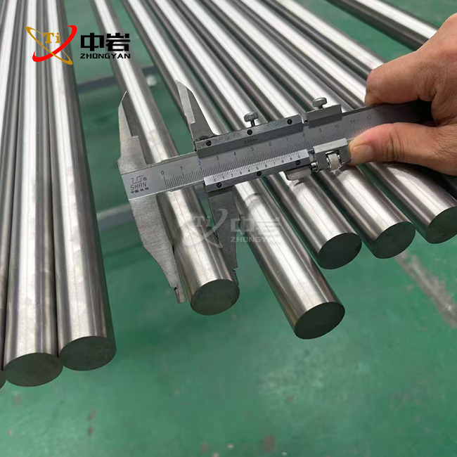
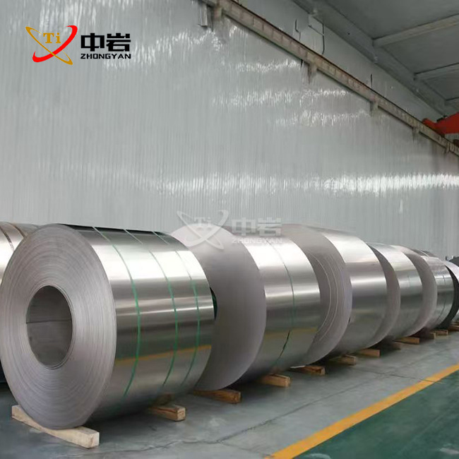
Planar titanium targets are manufactured using high-purity titanium, typically Grade 1 or Grade 2, to ensure the best possible film quality. The purity of these targets is crucial, often exceeding 99.995%, as even trace impurities can significantly affect the properties of the deposited films. The first step in making something is carefully choosing the raw titanium materials. These materials then go through strict cleaning processes to get rid of any impurities. Titanium is refined even more, and the right amount of clarity is reached by using advanced melting methods like electron beam melting or vacuum arc remelting. The bars that are made are then put through different steps, such as casting, rolling, and annealing, to get the best microstructure for sputtering uses. Strict quality control measures are used throughout this process to make sure that the flat titanium targets stay very pure and consistent.
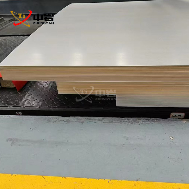
Once the high-purity titanium material is prepared, the planar targets undergo precision machining to achieve the required dimensions and surface characteristics. CNC machining is typically employed to ensure exceptional flatness and uniformity across the target surface. For constant sputtering rates and layer thickness during deposition processes, this level of accuracy is very important. Planar titanium targets have a carefully managed surface finish, with roughness values (Ra) of 0.4μm or less being the norm. This smooth surface helps keep particles from being made during sputtering, which makes the formed films better overall. Different surface processes can also be used to improve the target's performance or meet unique customer needs. Different sparking systems and application needs can be met by customizing the cutting process to fit a wide range of sizes and thicknesses.
Applications and Advantages
Rigorous quality control measures are implemented throughout the manufacturing process of planar titanium targets to ensure consistency and reliability. Advanced analytical techniques, such as inductively coupled plasma mass spectrometry (ICP-MS) and glow discharge mass spectrometry (GDMS), are used to verify the purity and composition of the targets. Non-destructive testing methods, including ultrasonic scanning and X-ray diffraction, are employed to detect any internal defects or variations in crystal structure. Each target undergoes thorough dimensional checks and surface inspections to confirm compliance with specifications. Proper packaging is crucial to protect the high-quality planar titanium targets during storage and transportation. Targets are typically vacuum-sealed in protective materials to prevent contamination and oxidation. For customers requiring OEM solutions, custom packaging and branding options are often available, allowing for seamless integration into their production processes.
In the semiconductor and electronics industries, planar titanium targets are very important because they are used to cast thin titanium films that are used for many things. When making integrated circuits, titanium layers help different materials stick together and stop them from moving around. The high purity of these targets ensures that there is little contamination, which is very important for keeping semiconductor devices' electrical features and dependability. Planar targets are used to cast titanium films, which are then used to make thin-film transistors for screens and microelectromechanical systems (MEMS). The steady performance of these electrical parts is helped by the regular sputtering properties of planar titanium targets. Because the sizes of the targets can be changed, they can work with a lot of different types of sputtering tools. This makes planar titanium targets a flexible option for many semiconductor manufacturing processes.
Optical Coatings and Solar Cells
In the field of optical coatings, planar titanium targets are extensively used to create high-performance thin films for various applications. Titanium dioxide (TiO2) coatings, produced by reactive sputtering of titanium targets in an oxygen environment, are widely used for anti-reflective and high-refractive-index layers in optical components such as lenses, mirrors, and filters. These coatings make the surfaces better at reflecting light and last longer, which makes them perfect for use in cameras, binoculars, and other optical tools. Titanium-based coatings put on with flat targets have more than one use in the solar cell business. They can be used as anti-reflective layers to help light pass through, as active layers in some cell designs, or as protective coats to make solar panels last longer. It is easier to use and more reliable for these optical and solar uses because flat titanium targets are very pure and sputter evenly.
Planar titanium targets are used a lot in many different industries to create and progress new materials and finishes. In the aircraft industry, coatings made of titanium that are applied using these targets protect parts that are exposed to harsh conditions, like the blades of jet engines. The coats make the parts of an airplane last longer and work better by making them less likely to wear out, protecting against rust, and blocking heat. TiN coatings, which are made by reactive sputtering titanium targets, are used a lot in the metalworking industry to make cutting tools and machine parts harder and less likely to break down. Plans made of titanium are also useful in medicine, where they are used to make coatings that are safe for medical tools and gadgets. Plans for titanium targets are great for making a lot of different shapes out of titanium. Because of this, they are very helpful for making new things that are better in every way.
Conclusion
Planar titanium targets are indispensable components in modern thin-film deposition processes, offering high purity, precision, and versatility across various industries. Their applications range from semiconductor manufacturing to optical coatings and advanced materials development. As a leading manufacturer, Zhong Yan Titanium excels in producing custom CNC-machined parts and titanium materials with high quality, precision, and volume. Our comprehensive services include CNC machining, material processing, and the production of various titanium products. Located in Baoji city, China's Titanium Valley, we leverage rich resources and advanced research to provide superior titanium solutions worldwide. For inquiries or custom requirements, please contact us at sales@titaniumstudy.com.
FAQ
Q: What is the typical purity of planar titanium targets?
A: Planar titanium targets typically have a purity of 99.995% or higher.
Q: Can planar titanium targets be customized for specific sputtering systems?
A: Yes, planar titanium targets can be customized in terms of size, thickness, and bonding options to fit various sputtering systems.
Q: What industries primarily use planar titanium targets?
A: The main industries using planar titanium targets include semiconductors, optics, solar cells, and aerospace.
Q: How are planar titanium targets manufactured to ensure high quality?
A: The manufacturing process involves high-purity raw material selection, advanced melting techniques, precision machining, and rigorous quality control measures.
Q: What are some common applications of titanium films deposited using planar targets?
A: Common applications include adhesion layers in semiconductors, anti-reflective coatings in optics, and wear-resistant coatings for tools and aerospace components.
References
1. Smith, J.R. (2018). "Advances in Planar Sputtering Targets for Thin Film Deposition". Journal of Vacuum Science & Technology A, 36(5), 050801.
2. Johnson, M.K., & Brown, L.T. (2019). "High-Purity Titanium Targets for Semiconductor Applications". Thin Solid Films, 677, 78-85.
3. Lee, C.H., et al. (2020). "Optimization of Planar Titanium Target Properties for Enhanced Sputtering Performance". Surface and Coatings Technology, 386, 125470.
4. Wang, Y., & Liu, Z. (2017). "Microstructure Control in Titanium Sputtering Targets: Effects on Film Quality". Materials Science and Engineering: B, 225, 53-60.
5. Garcia-Alonso, M.C., et al. (2021). "Planar Titanium Targets for Biomedical Coatings: Current Status and Future Perspectives". Biomaterials Science, 9(15), 5132-5148.
6. Thompson, R.D. (2016). "Manufacturing Processes for High-Performance Sputtering Targets". In Advanced Materials for Thin Film Deposition (pp. 123-150). Springer, Cham.
_1755652433231.jpg)
Learn about our latest products and discounts through SMS or email